HOTLINE: +84 979761016
Force and mechanical measuring equipment
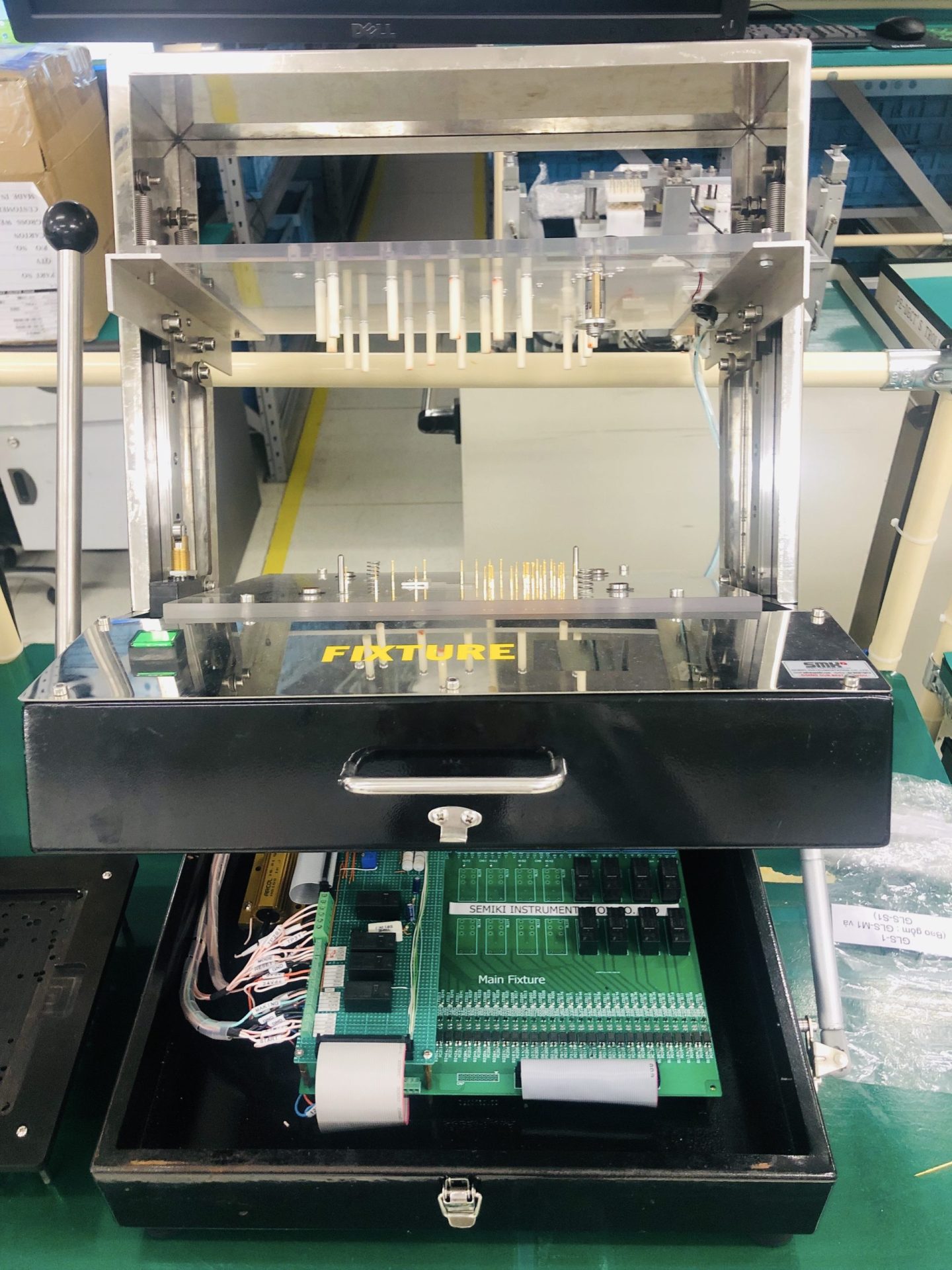
SEMIKI-PCBA Functional Testing Fixtures
Many different test fixtures have been developed for functional testing of a PCBA (PCB assembly). Electrical connections may be made with connectors present on the PCBA or by test probes that contact test points defined by the PCB designer. Connectors on a test fixture are usually modified to allow for ease of mating and de-mating of the fixture's connectors and the connectors on the PCBA to be tested. Connectors and the connectors on the PCBA to be tested. Connectors on the test fixture are also usually made easily replaceable, since they can wear out quickly with the multiple mating and de-mating cycles of production testing.

Semiki
Test Jig/test fixture for PCBA Testing
► PCBA Functional Testing Fixtures
Many different test fixtures have been developed for functional testing of a PCBA (PCB assembly). Electrical connections may be made with connectors present on the PCBA or by test probes that contact test points defined by the PCB designer. Connectors on a test fixture are usually modified to allow for ease of mating and de-mating of the fixture's connectors and the connectors on the PCBA to be tested. Connectors and the connectors on the PCBA to be tested. Connectors on the test fixture are also usually made easily replaceable, since they can wear out quickly with the multiple mating and de-mating cycles of production testing.
When making direct contact to test points on a PCBA, probes under the PCBA are typically fixed and the test fixture applies hold-down force to the top of the PCBA for reliable electrical connections to the test probes. If the PCBA being tested has test points on both sides of the board, then two probe plates are required, both of which must be precisely aligned to each other and to the PCBA under test. With double-sided probing, the PCBA under test is typically fixed in place and the probes move in from both top and bottom when the fixture is operated.
You can use the following checklist to help ensure that your PCB designs are testable:
• At least 1 test point is available on each net that you would like to test.
• Use 1mm or greater diameter pads that are not covered with solder paste for each test point.
• Place test points at distance of >1.91mm from each other.
• Place all test points on either the top or bottom of the PCB board. Preferably, place them on the least populated side of the board.

► Semiki is one of the prominent manufacturers/suppliers for ICT/FCT Test Jigs & Function Test Jigs.
We have a dedicated team of experienced engineers for ICT/ FCT Test Jigs development & technical support including pin fixture development, fabrication & debugging.
Our fixture house has the capacity to develop 10 to 30 Jigs / Month.
• We manufacture jigs using our hand press unit.
• We are confident in the quality because we manufacture jigs after knowing all about the hand press unit.
• All jig parts are standardized, and it is possible to manufacture with short delivery time and low price.
• As a pioneer in jig manufacturing, Semiki has been highly evaluated by domestic and overseas customers.
• We can respond to customer needs, such as manufacturing only the pin board part (wiring work by the customer) and assembling / wiring work of the control board.

► With our Semiki service, test jig removes roadblocks and headaches that firmware developers and hardware designers encounter daily. There is no longer a need to solder power cables or programming headers to PCBA's and no more debugging of loose connections and broken solder joints. PCBA functional tests can be developed earlier and in less time by reducing the time needed to design a production capable fixture.

Test Jig File Requirement
Test Jig fabrication requires ECAD files to automatically identify test points, mounting holes, and other test features. We support the following file formats:
Altium Test Point Reports (.csv)
Eagle (.brd)
Gerbers (.zip)
KiCAD (.kicad_pcb)
Test Jig Design
Choose test probe card and receptable types from a list of parts that are compatible with the fixture. Add, modify, and remove probes and guide pins as needed. DUT (device under test) location and panelization settings can also be configured, allowing for the fixture to test an entire panel at a time. Visually review a generated jig before finalizing the design.
Test Jig Fabrication
Download the Design File Package which includes everything needed to build the fixture. Use the files to fabricate the plates using Acrylic, CNC milling or laser cutting.
Test Jig Assembly
Attach all probes and guild pins, integrate your test instrumentation, and run your test
Design for Test (DFT)
Building a test fixture can be a difficult and costly process, especially if the PCB wasn't designed with test in mind. The following tips can help make testing your PCB assemblies much easier when using a bed-of-nails style test fixture (/jig).
Single-sided Probing
All test points should be placed on a single side of the PCB, preferring the side with fewer components. This will greatly reduce the cost and complexity of the test fixture required to test the PCB board in rigid and flex.
Test Point Grid Spacing
A common term in the PCBA testing world is Test Point Grid Spacing. This means the minimum space between test points on the PCB and is defined using either mil (a thousandth of an inch) or mm. Test probes come in a variety of grid spacings, with the most common being:
P100 (100mil or 2.54mm spacing)
P75 (75mil or 1.91mm spacing)
P50 (50mil or 1.27mm spacing)
Test Probe and Test Point Types
While different types of test points and probes can be used, we recommend using regular pads with a minimum diameter of 0.8mm (31.5mil). These can easily be accessed by most probe types. Increasing the pad diameter to 1mm will help improve the reliability of the tester. Different test point types and the test probes that should be used are described below.
Leads
A lead test point is created by the lead from a through-hole component that is soldered to the PCB board. Serrated probe tips usually have the longest life, but cupped probe tips can also be used.
Terminals and Posts
A terminal or post is created by a component with a square terminal or post that is soldered to the PCB. These types of test points are best contacted by slotted (self-cleaning) cups when used facing upwards. Serrated or flat tips will also work. However, the cup tips will self-align to the terminals or post.

* The Most Trusted Name in Research
– SEMIKI Measurement Solution systems offer a highly efficient platform for bridging the gap between advanced theoretical and algorithm framework and real-world implementation.
– SEMIKI is happy to share Technical and Solutions relating to metrology, measuring, precision gages, manufacturing quality control and processes.
Call us today and see for yourself! There are lots more of us “behind the scenes”
Office Phone : ( +84) 28 2253 3522
Hotline Phone: (+84) 9797 61016
Email : sales@semiki.com
~DOING OUR BEST FOR YOU~

SEMIKI measurement solution, PCB function tester

PCB function tester, Chip loading machine

PCB function tester

PCB function tester

PCB function tester

PCB function tester, Chip loading machine

PCB function tester

PCB function tester